Catchcam: Designing GNSS Circuitry
In this post, I will discuss the design and implementation of the GNSS circuitry for my Catchcam project.
If you haven’t already, I recommend reading my previous post on Catchcam: Choosing Components to get some background on the component selection process. In that post, I discussed my decision to use the SIM68M GNSS module and the KH-GPS252504-WY Ceramic Patch antenna for my project. In this post, I’ll dive deeper into the design and implementation of the GNSS circuitry.
Note: If you’re interested, you can pre-order a sample at vnucec.ivan@gmail.com.
GNSS Module
SIM68M is quite a simple GNSS module. It is powered by a 3.3V supply, has a built-in LNA, supports both active and passive antennas, and communicates over UART using the NMEA protocol.
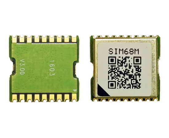
However, I’ve encountered a couple of issues during implementation.
The datasheet specified a baud rate of 115200 (see the image below), but in reality, the module operated at 9200 baud. However, this was not a big issue, because the baud rate can be easily configured by sending the appropriate AT command over UART.

Additionally, the datasheet lacked information about the part orientation in the reel, leading to assembly problems at JLCPCB. I’ve had to opt for manual inspection option, which added a small extra cost. Other than that, I am quite pleased with the performance of the module.
Antenna
I’ve decided to go with the 25x25 mm KH-GPS252504-WY GNSS antenna.
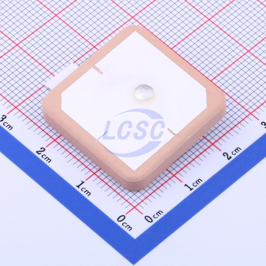
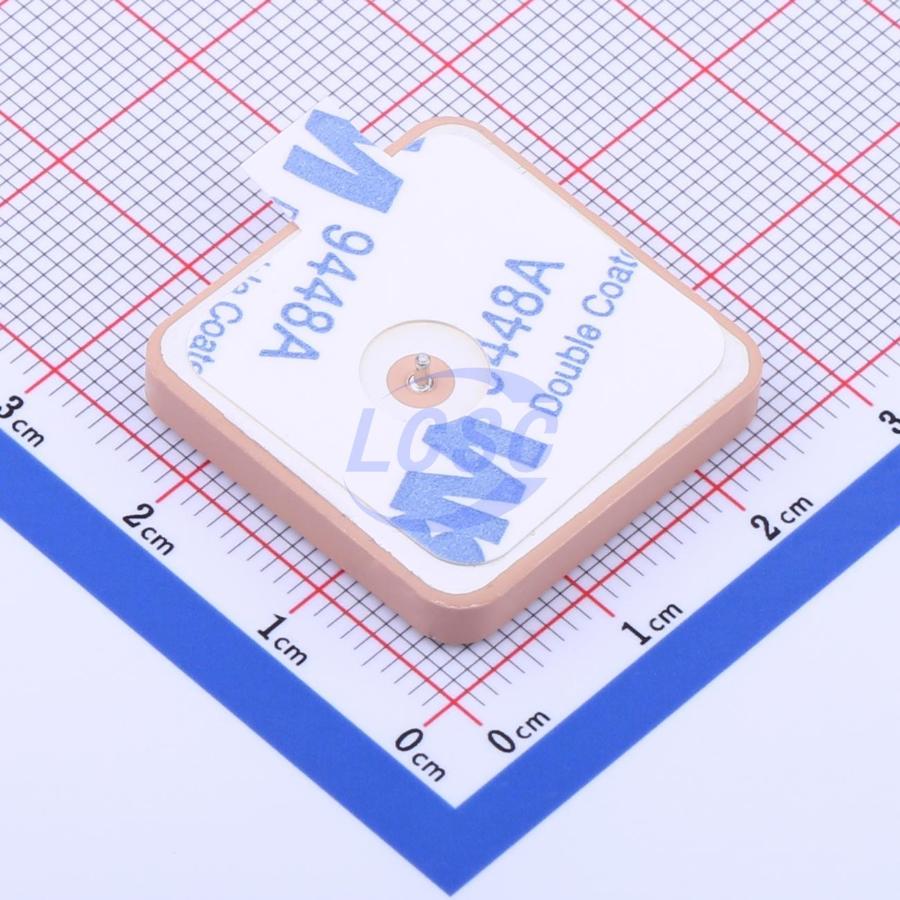
It was really cheap one, although the datasheet is a bit lacking when it comes to the recommended ground plane size (more on that later). I reached out to the manufacturer for some clarity, and their customer support was surprisingly helpful. They told me a 60x60 mm ground plane would do the trick, but they didn’t really explain why. Still, they were generous enough to offer 10 free samples for our project, which was a nice gesture.
PCB Design
I’ve chosen GND - SIG/PWR - SIG/PWR - GND stackup for my 4-layer PCB because the GNSS Antenna needs a solid ground plane beneath it to work properly. Antenna is placed on the top side, while the GNSS module and the rest of the system circuitry is placed on the bottom side. This way, the antenna feed pin is as close as possible to the module in order to minimize PCB signal loss and interference. The stackup I’ve chosen is not ideal because the inner signals are not shielded by the ground planes as they would be in a more popular SIG/PWR - GND - GND -SIG/PWR stackup. The ground size is set to 60x60 mm, as recommended by the antenna manufacturer.
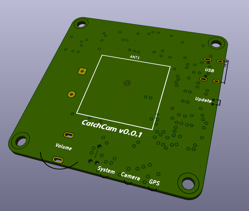
I couldn’t manage to get 50 Ohm impedance on the GNSS signal trace with the chosen stackup (they were exceeding 1 mm in width), but I’m not too worried about it because the trace lengths are much shorter than the GNSS signal wavelength. I’ve also added a Pi matching network footprints to the PCB, and added 0 Ohm resistor so I can to tune the signal trace later.
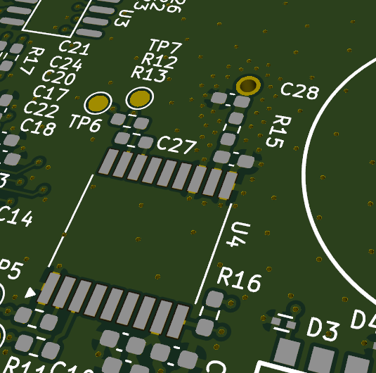
I’ve spaced out any other trace or component that might potentially interfere with the GNSS signal. I’ve surrounded the GNSS signal trace with lots of ground stitching vias to create a signal waveguide in order to minimize interference.
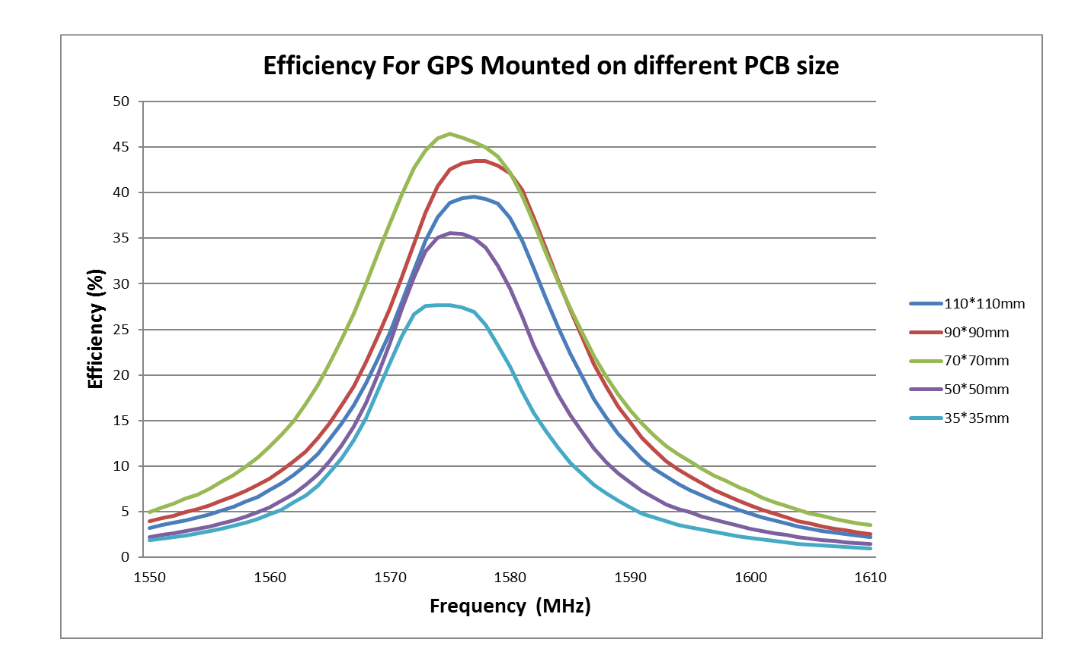
Note that the antenna resonant frequency (and efficiency) shifts with different ground plane sizes as shown in this Application specification, and depending on the size of the antenna and the PCB, there is a sweet spot where the antenna efficiency is the highest. In my case, I had to guess because the datasheet didn’t provide any information on the ground plane size.
I would like to mention a nRF9161-dk reference design, which was quite helpful in designing the GNSS circuitry. Also, the ANR017 GNSS ANTENNA SELECTION guide helped me understand that the best way to place a GNSS antenna is in the middle of the PCB and with a solid ground plane beneath it.
Testing
Antenna performance
After the boards arrived, I’ve measured the antenna characteristics using the MegiQ VNA-0460 VNA by soldering a coaxial cable to the antenna feed pin.
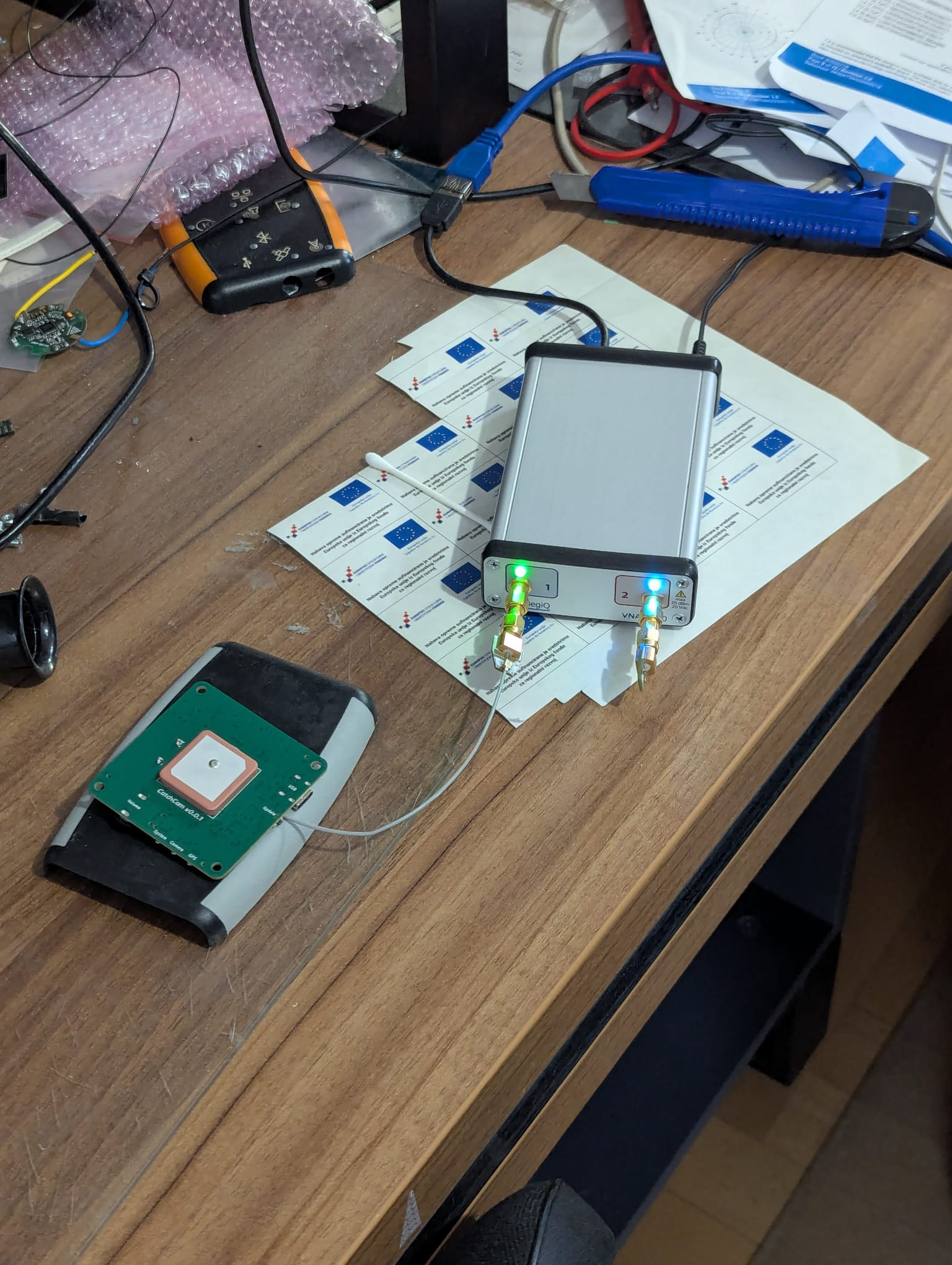
The results were quite promising as you can see in the images below (note that the GNSS L1 band is grayed out).
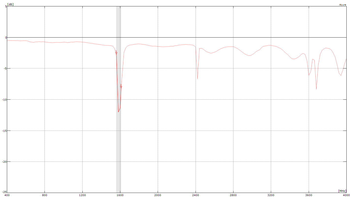
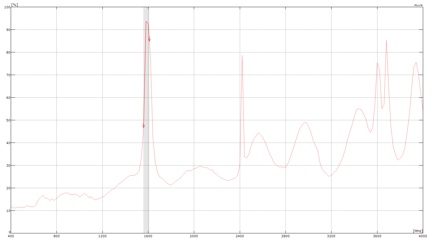
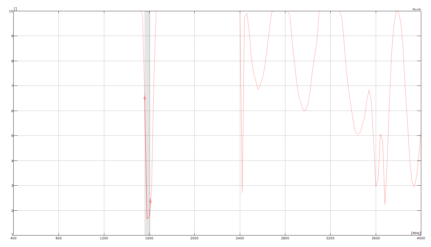
Antenna has a return loss at around -12 dB, which is quite good. The efficiency is around 93% at the resonant frequency, which is also quite good. The VSWR is around 1.6. Overall, I’m quite pleased with results even without the matching network components populated.
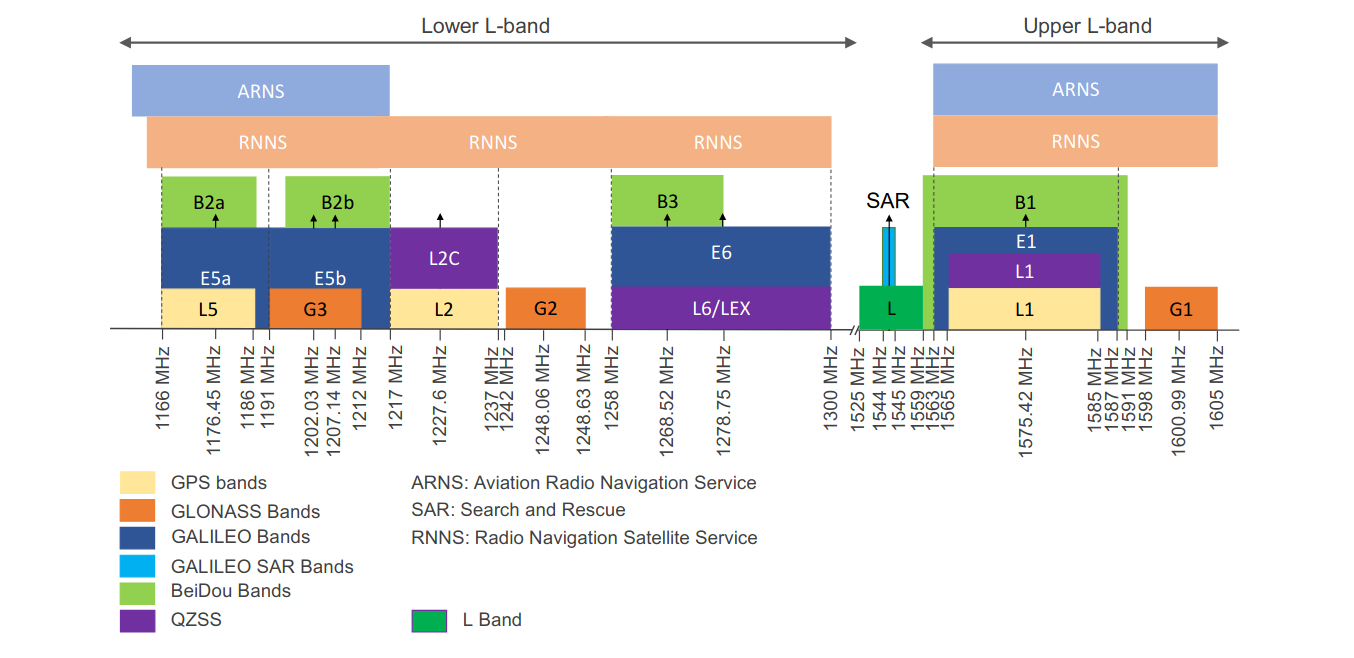
The grayed out area is the GNSS L1 band, which is the frequency range where the most popular GNSS systems operate. The image below shows the GNSS upper and lower bands with the L1 band to the right.
We’ve also calculated the matching network components values using MegiQ VNA software, but since I’m quite pleased with the antenna characteristics, I’ve decided not to populate them and leave the 0 Ohm resistors in place.
GNSS Module performance
Using GNSS module, the Time-to-first-fix upon cold-start was around 30 seconds under the open sky, which is close to the specified time in the datasheet.

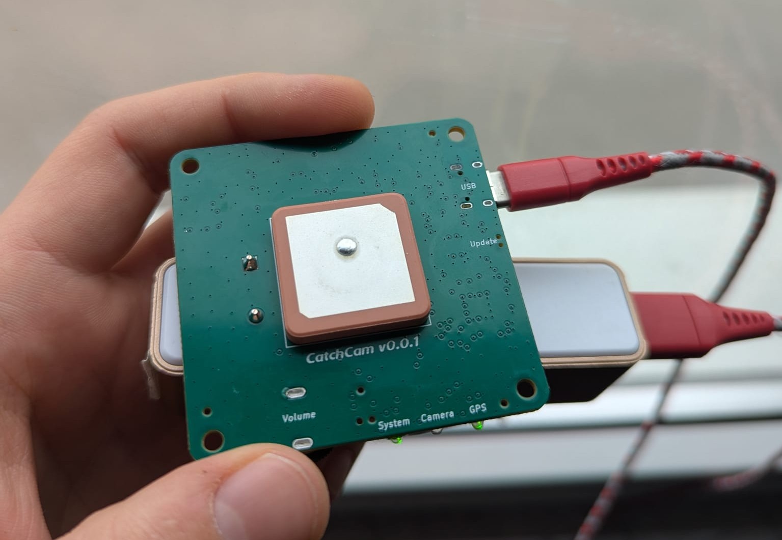
The module was able to maintain a fix even in the middle of a room with no windows, which is quite impressive. Also, the module was able to get a fix when placed on a car seat, so they don’t need to be placed on the car dashboard, which is a plus in our case.
Conclusion and Future considerations
Overall, I’m really satisfied with the GNSS circuitry design and implementation, however there are a couple of things I would like to improve in the future.
I want to replace SIM68M module with a cheaper one. Currently, the price of the module is around $7.5 per unit, which places it as the most expensive component on the board, and I’ve seen 2x cheaper modules with similar performance on the market.
Also, I would like to experiment with different ground plane sizes to see how it affects the antenna performance. I would also like to try the smaller active antenna to see if we can reduce the board size.
Thank you for reading this post. If you have any questions or suggestions, feel free to leave a comment below. Stay tuned for more updates on the Catchcam project.
Note: If you’re interested, you can pre-order a sample at vnucec.ivan@gmail.com.
